Outils pour utilisateurs
Table des matières
8253/8254 PIT - Programmable Interval Timer
The Intel 8253 and 8254 are programmable interval timers (PITs), which perform timing and counting functions using three 16-bit counters.
The 825x family was primarily designed for the Intel 8080/8085-processors, but were later used in x86 compatible systems. The 825x chips, or an equivalent circuit embedded in a larger chip, are found in all IBM PC compatibles.
In PC compatibles, Timer Channel 0 is assigned to IRQ-0 (the highest priority hardware interrupt). Timer Channel 1 is assigned to DRAM refresh (at least in early models before the 80386). Timer Channel 2 is assigned to the PC speaker.
The Intel 82c54 (c for CMOS logic) variant handles up to 10 MHz clock signals.
Features of 8253 / 8254
The most prominent features of 8253/8254 are as follows:
- It has three independent 16-bit down counters.
- It can handle clock up to 2.6 MHz (10 MHz for the 8254).
- These three counters can be programmed for either binary or BCD count.
- It is compatible with almost all microprocessors.
- 8254 has a powerful command called READ BACK command, which allows the user to check the count value, the programmed mode, the current mode, and the current status of the counter.
8253/8254 IBM PC Ports description
| Port | Model | Description |
|---|---|---|
| 40h | 8253 | Counter 0 Time of Day Clock (normally mode 3) |
| 41h | 8253 | Counter 1 RAM Refresh Counter (normally mode 2) |
| 42h | 8253 | Counter 2 Cassette and Speaker Functions |
| 43h | 8253 | Mode Control Register, data format (see below) |
| 44h | 8254 | PS/2 extended timer |
| 47h | 8254 | Channel 3 control byte |
Port 43h
Bits 0 - Counter format
Bits 1-3 - Counter Mode Bits
| Bits | |
|---|---|
| 000 | mode 0, interrupt on terminal count; countdown, interrupt, then wait for a new mode or count; loading a new count in the middle of a count stops the countdown |
| 001 | mode 1, programmable one-shot; countdown with optional restart; reloading the counter will not affect the countdown until after the following trigger |
| 010 | mode 2, rate generator; generate one pulse after 'count' CLK cycles; output remains high until after the new countdown has begun; reloading the count mid-period does not take affect until after the period |
| 011 | mode 3, square wave rate generator; generate one pulse after 'count' CLK cycles; output remains high until 1/2 of the next countdown; it does this by decrementing by 2 until zero, at which time it lowers the output signal, reloads the counter and counts down again until interrupting at 0; reloading the count mid-period does not take affect until after the period |
| 100 | mode 4, software triggered strobe; countdown with output high until counter zero; at zero output goes low for one CLK period; countdown is triggered by loading counter; reloading counter takes effect on next CLK pulse |
| 101 | mode 5, hardware triggered strobe; countdown after triggering with output high until counter zero; at zero output goes low for one CLK period |
The 1-3 bits of the control word set the operating mode of the timer. There are 6 modes in total
For modes 2 and 3, the bit 3 is ignored, so the missing modes 6 and 7 are aliases for modes 2 and 3.
The OUT signal is linked to CPU (via Interrupt).
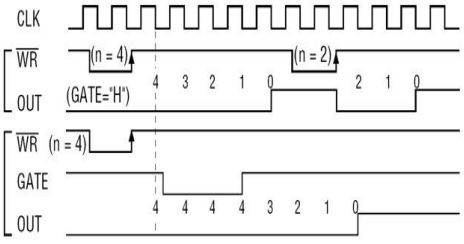
Mode 0 (000): Interrupt on terminal count
Mode 0 is used for the generation of accurate time delay under software control. In this mode, the counter will start counting from the initial COUNT value loaded into it, down to 0. Counting rate is equal to the input clock frequency.
The OUT pin is set low after the Control Word is written, and counting starts one clock cycle after the COUNT is programmed. OUT remains low until the counter reaches 0, at which point OUT will be set high until the counter is reloaded or the Control Word is written. The counter wraps around to 0xFFFF internally and continues counting, but the OUT pin never changes again. The Gate signal should remain active high for normal counting. If Gate goes low, counting is suspended, and resumes when it goes high again.
The first byte of the new count when loaded in the count register, stops the previous count.
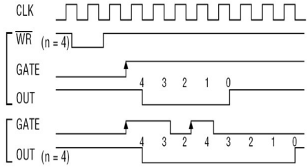
Mode 1 (001): programmable one shot
In this mode 8253 can be used as a monostable multivibrator. GATE input is used as trigger input.
OUT will be initially high. OUT will go low on the Clock pulse following a trigger to begin the one-shot pulse, and will remain low until the Counter reaches zero. OUT will then go high and remain high until the CLK pulse after the next trigger.
After writing the Control Word and initial count, the Counter is armed. A trigger results in loading the Counter and setting OUT low on the next CLK pulse, thus starting the one-shot pulse. An initial count of N will result in a one-shot pulse N CLK cycles in duration.
The one-shot is retriggerable, hence OUT will remain low for CLK pulses after any trigger. The one-shot pulse can be repeated without rewriting the same count into the counter. GATE has no effect on OUT. If a new count is written to the Counter during a oneshot pulse, the current one-shot is not affected unless the counter is retriggered. In that case, the Counter is loaded with the new count and the oneshot pulse continues until the new count expires.
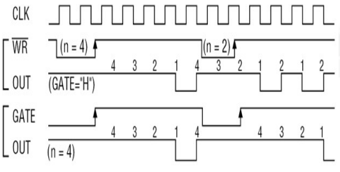
Mode 2 (X10): rate generator
In this mode, the device acts as a divide-by-n counter, which is commonly used to generate a real-time clock interrupt.
Like other modes, the counting process will start the next clock cycle after COUNT is sent. OUT will then remain high until the counter reaches 1, and will go low for one clock pulse. The following cycle, the count is reloaded, OUT goes high again, and the whole process repeats itself.
The time between the high pulses depends on the preset count in the counter's register, and is calculated using the following formula:
Note that the values in the COUNT register range from to 1; the register never reaches zero.
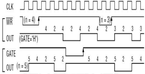
Mode 3 (X11): square wave generator
This mode is similar to mode 2. However, the duration of the high and low clock pulses of the output will be different from mode 2.
Suppose is the number loaded into the counter (the COUNT message), the output will be high for
counts, and low for
counts. Thus, the period will be
counts, and if
is odd, the extra half-cycle is spent with OUT high.
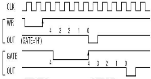
Mode 4 (100): Software Triggered Strobe
After Control Word and COUNT is loaded, the output will remain high until the counter reaches zero. The counter will then generate a low pulse for 1 clock cycle (a strobe) – after that the output will become high again.
GATE low suspends the count, which resumes when GATE goes high again.
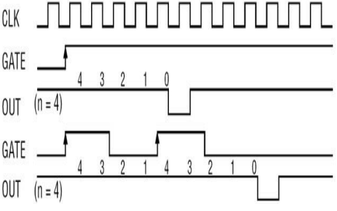
Mode 5 (101): Hardware Triggered Strobe
This mode is similar to mode 4. However, the counting process is triggered by the GATE input.
After receiving the Control Word and COUNT, the output will be set high. Once the device detects a rising edge on the GATE input, it will start counting. When the counter reaches 0, the output will go low for one clock cycle – after that it will become high again, to repeat the cycle on the next rising edge of GATE.
Bits 4-5 - Read/Write/Latch Format Bits
| Bits | |
|---|---|
| 00 | latch present counter value |
| 01 | read/write of MSB only |
| 10 | read/write of LSB only |
| 11 | read/write LSB, followed by write of MSB |
Bits 6-7 - Counter Select Bits
| Bits | |
|---|---|
| 00 | select counter 0 |
| 01 | select counter 1 |
| 10 | select counter 2 |
| 11 | read back command (8254 only, illegal on 8253, see below) |
Read Back Command Status (8254 only)
| Bit | Read Back Command Status |
|---|---|
| 0 | 0=16 binary counter 1=4 decade BCD counter |
| 1-3 | counter mode bits (see Mode Control Reg above) |
| 4-5 | read/write/latch format (see Mode Control Reg) |
| 6 | 1=null count (no count set) 0=count available |
| 7 | state of OUT pin (1=high, 0=low) |
- the 8253 is used on the PC & XT, while the 8254 is used on the AT+
- all counters are decrementing and fully independent
- the PIT is tied to 3 clock lines all generating 1.19318 MHz.
- the value of 1.19318MHz is derived from (4.77/4 MHz) and has it's roots based on NTSC frequencies
- counters are 16 bit quantities which are decremented and then tested against zero.Valid range is (0-65535). To get a value of 65536 clocks you must specify 0 as the default count since 65536 is a 17 bit value.
- reading by latching the count doesn't disturb the countdown but reading the port directly does; except when using the 8254 Read Back Command
- counter 0 is the time of day interrupt and is generated approximately 18.2 times per sec. The value 18.2 is derived from the frequency 1.10318/65536 (the normal default count).
- counter 1 is normally set to 18 (dec.) and signals the 8237 to do a RAM refresh approximately every 15ms
- counter 2 is normally used to generate tones from the speaker but can be used as a regular counter when used in conjunction with the 8255
- newly loaded counters don't take effect until after a an output pulse or input CLK cycle depending on the mode
- the 8253 has a max input clock rate of 2.6MHz, the 8254 has max input clock rate of 10MHz
Programming considerations:
- load Mode Control Register
- let bus settle (jmp $+2)
- write counter value
- if counter 0 is modified, an INT 8 handler must be written to call the original INT 8 handler every 18.2 seconds. When it does call the original INT 8 handler it must NOT send and EOI to the 8259 for the timer interrupt, since the original INT 8 handler will send the EOI also.
Example code:
countdown  equ	8000h 	; approx 36 interrupts per second

   cli
   mov  al,00110110b	; bit 7,6 = (00) timer counter 0
			; bit 5,4 = (11) write LSB then MSB
			; bit 3-1 = (011) generate square wave
			; bit 0 = (0) binary counter
   out	43h,al  	; prep PIT, counter 0, square wave&init count
   jmp	$+2		; wait/sync
   mov	cx,countdown  	; default is 0x0000 (65536) (18.2 per sec)
			; interrupts when counter decrements to 0
   mov	al,cl		; send LSB of timer count
   out	40h,al
   jmp	$+2		; wait/sync
   mov	al,ch		; send MSB of timer count
   out	40h,al
   jmp	$+2		; wait/sync
   sti
Hardware informations
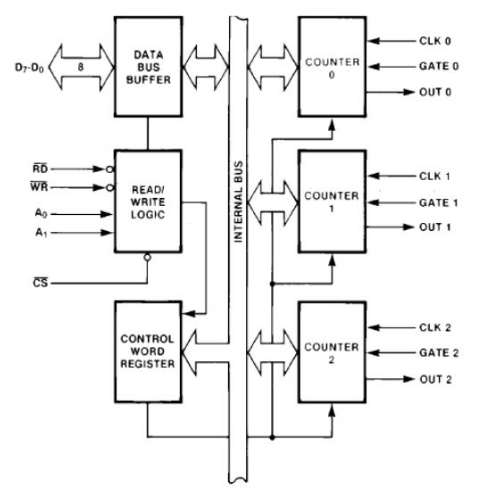
8254 Architecture
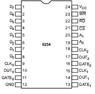
8254 Pin Description
Here is the pin diagram of 8254 −
In the above figure, there are three counters, a data bus buffer, Read/Write control logic, and a control register. Each counter has two input signals - CLOCK & GATE, and one output signal - OUT.
Data Bus Buffer
It is a tri-state, bi-directional, 8-bit buffer, which is used to interface the 8253/54 to the system data bus. It has three basic functions:
- Programming the modes of 8253/54.
- Loading the count registers.
- Reading the count values.
Read/Write Logic
It includes 5 signals, i.e. RD, WR, CS, and the address lines A0 & A1. In the peripheral I/O mode, the RD and WR signals are connected to IOR and IOW, respectively. In the memorymapped I/O mode, these are connected to MEMR and MEMW.
Address lines A0 & A1 of the CPU are connected to lines A0 and A1 of the 8253/54, and CS is tied to a decoded address. The control word register and counters are selected according to the signals on lines A0 & A1.

